Objective: In this lab exercise, you will use Verilog hardware description language to design and simulate a register file, which will be used in later lab exercises. Verilog design provides an alternative to the register file in schematic.
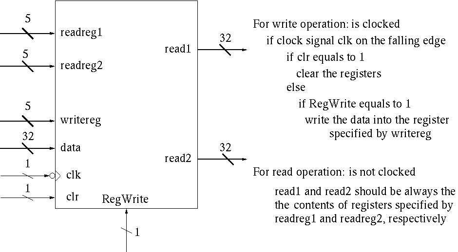
Register File Specification: A register file consists of thirty-two 32-bit registers that can be read and written by supplying a register number to be accessed. The figure 1 and figure 2 show you a draft schematic of the register file. The register file with two read ports and one write port has five inputs (Read register number 1, Read register number 2, Write register, Write data, and Write control), and two outputs (Read data 1 and Read data 2). Each of Read register number 1 (readreg1), Read register number 2 (readreg2), and Write register (writereg) is used to specify one of the 32 registers for either reading or writing. The register file also has clock signal input clk and clear signal input clr.
The write operation takes place on the falling edge of the clk signal when the Write control (RegWrite) is logical 1. The read operation, however, is not clocked - it is combinational. Thus, the value of Read data 1 (read1) should always be the contents of the register specified by the Read register number 1. Similarly, the value of Read data 2 (read2) should always be the contents of the register specified by the Read register number 2. The following figure and table give the description of the register file. The table only describes the cases when clear signal clr is 0. When the clear signal clr is 1, clear the registers.
| Input | Inside of the register file | Output | ||||||
| clk | RegWrite | readreg1 | readreg2 | writereg | data | registers 0~31 | read1 | read2 |
| register no. 1 | read the data from the register specified by readreg1 | |||||||
| register no. 2 | read the data from the the register specified by readreg2 | |||||||
 |
0 | data | no change | |||||
|
1 | register no. | data | write data into the register specified by writereg |
Lab Requirements:
Help for Sequential LogicVerilog:
Read the Verilog code of positive (rising) edge-triggered D flip-flop with asynchronous clear and Verilog code of negative (falling) edge-triggered D flip-flop with asynchronous clear. The module and its inputs and outputs are declared. q is declared as of type reg since it will store information. The process begins with the keyword always. Following is @(posedge clock or posedge clear). The @ operator can be viewed as "wait for event." This is the event control statement for the process that initiates process execution if an event, i.e., a specified change in a specified signal occurs. For the D flip-flop, if either clock or clear change, then the process is executed. It is important to note that the event control statement is not a parameter list containing all inputs. For example, data does not appear, since a change in its value cannot initiate a possible change in the value of data. Following the event control statement at the beginning of the process is the keyword begin, and at the end of the process the keyword end appears.
Within the body of the process, there are additional Verilog conditional structures that can appear. The general structure of an if-else in Verilog is:
if (condition) begin procedural statement endIf there is a single procedural statement, then the begin and end are unnecessary.
{else if (condition)
begin procedural statement end}
{else
begin procedural statement end}
The procedural statements are classified as blocking and non-blocking. Blocking assignments use = as the assignment operator and non-blocking assignments use <= as the operator. Blocking assignments are executed sequentially, much like a program in C programming language. Non-blocking assignments evaluate the right hand side, but do not make the assignment until all right hand sides have been evaluated.
Back to Exercise Page of Computer Architecture Course .